歡迎光臨~泰州巨納新能源有限公司
語言選擇:
 ∷
∷

∷
 ∷
∷


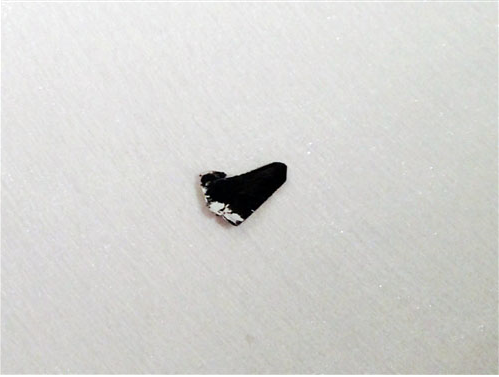
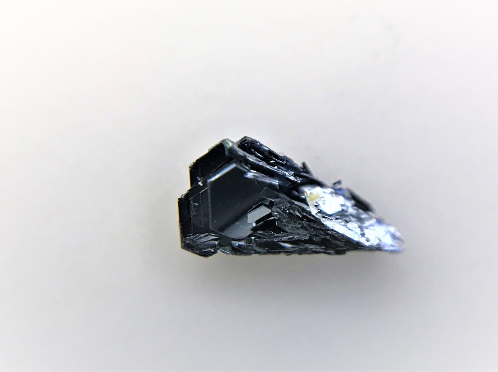
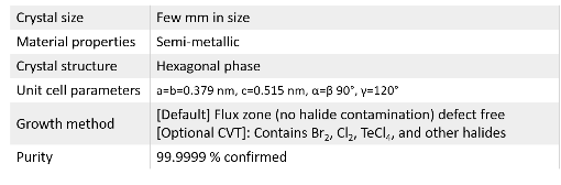
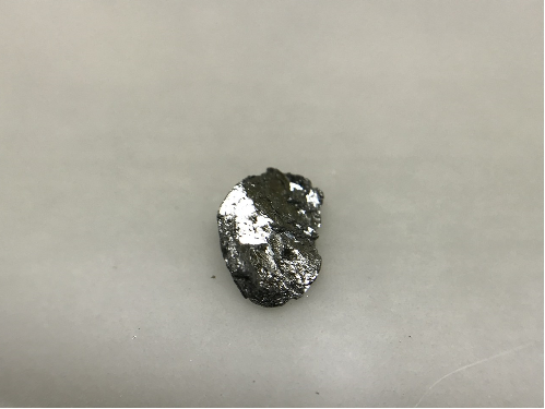
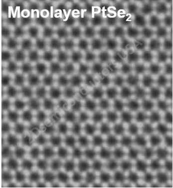
Platinum diselenide (PtSe2) is a member of transition metal dichalcogenide (TMDCs) family with the MX2 formula. While it is an established semimetal in the bulk form the band gap of its monolayer has been recently predicted to be a semiconductor (Nano Letters, 2015, 15, 4013).
Growth method matters> Flux zone or CVT growth method? Contamination of halides and point defects in layered crystals are well known cause for their reduced electronic mobility, poor e-h recombination, low-PL emission, and lower optical absorption. Flux zone technique is a halide free technique used for synthesizing truly semiconductor grade vdW crystals. This method distinguishes itself from chemical vapor transport (CVT) technique in the following regard: CVT is a quick (~2 weeks) growth method but exhibits poor crystalline quality and the defect concentration reaches to 1E11 to 1E12 cm-2 range. In contrast, flux method takes long (~3 months) growth time, but ensures slow crystallization for perfect atomic structuring, and impurity free crystal growth with defect concentration as low as 1E9 - 1E10 cm-2. So if your research needs truly high quality crystals for optoelectronics, scanning tunneling microscopy, spectroscopy, and other projects that rely on defect free crystals, flux zone growth is ideal for you. However, if you need catalytic materials presence of defects typically helps and in such case CVT method is better suited. During check out just state which type of growth process is preferred. Unless otherwise stated, 2Dsemiconductors ships Flux zone crystals as a default choice.
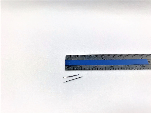
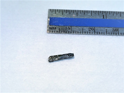
Properties of PtSe2 crystals by 2Dsemiconductors USA
聯系人:嚴春偉
手機:13914543285
電話:0523-86190619,86192878
郵箱:taizhou@sunano.com.cn
地址: 江蘇省泰州市鳳凰西路168號