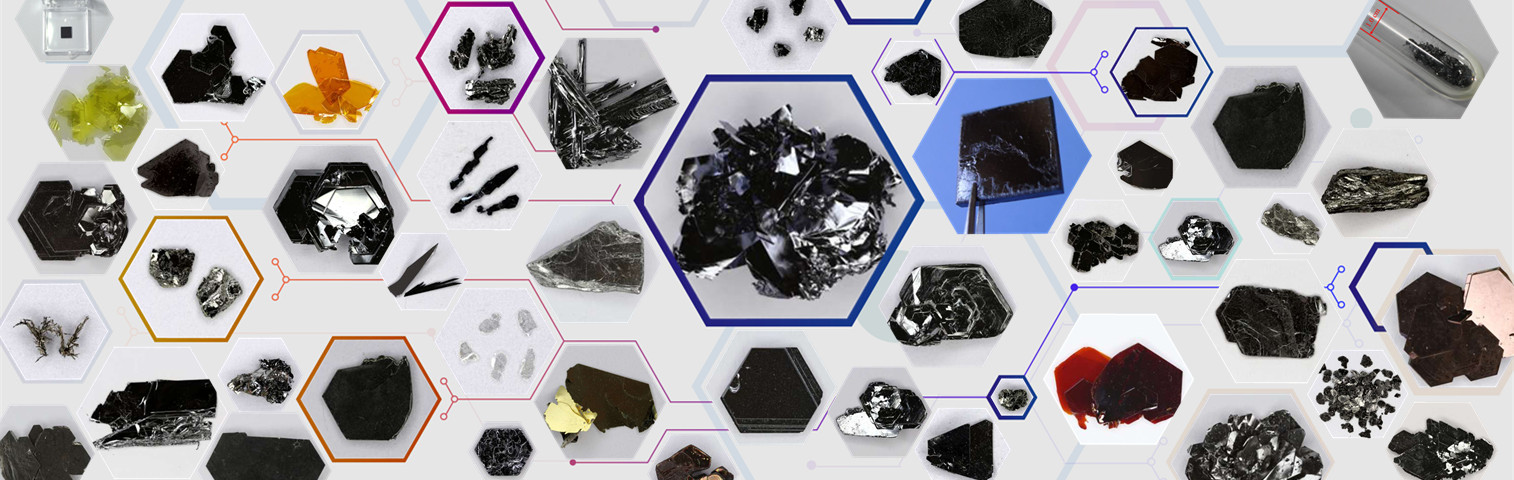
石墨烯粉末
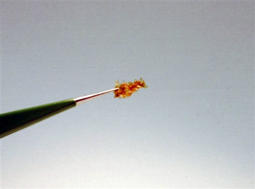
Semiconductor analog of graphene: Graphene oxide has been synthesized at our R&D facilities using modified reaction Hummer technique. Growth technique emphasizes on minimizing the defect density to yield optically active material and increasing the average grain size (flake size). Unlike many other graphene oxides, this product is optically active and is ready for 2D semiconductor research. Each growth batch has been characterized by Auger electron and x-ray photoelectron spectroscopy to determine the stoichometry; Raman, PL spectroscopy, and optical absorption for optical properties tests; AFM measurements for the atomic flatness. Product displays PL at ~2.5 eV, sub-bands at 2.2 and 2.0 eV, and broad defect lines at 1.7 eV. Raman spectroscopy measurements yield D, G, 2D, and G+D peaks. Samples come fully saturated with oxygen and the optical properties of the material can be tuned by simple heat treatment. The product is ideal for yielding monolayer onto various substrates within 2-10 minutes. Please contact us for more information.
 ∷
∷